Semiconductor device

a technology of semiconductors and devices, applied in semiconductor devices, semiconductor/solid-state device details, electrical equipment, etc., can solve the problems of fatigue failure in the joining portion of the lead frame (electrode lead) and fatigue failure in some cases, so as to reduce fatigue failure and relieve thermal stress

Active Publication Date: 2009-12-31
MITSUBISHI ELECTRIC CORP
View PDF5 Cites 5 Cited by
  • Summary
  • Abstract
  • Description
  • Claims
  • Application Information

AI Technical Summary

Benefits of technology

[0008]The present invention has been made in view of the above problems and an object thereof is to provide a semiconductor devi

Problems solved by technology

In the above power semiconductor device, however, in a case where the semiconductor device generates heat or the usage environment of the semiconductor device changes, fatigue failure due to thermal stress applied to a

Method used

View more

Image

Smart Image Click on the blue labels to locate them in the text.
Viewing Examples
Smart Image
  • Semiconductor device
  • Semiconductor device
  • Semiconductor device

Examples

Experimental program
Comparison scheme
Effect test

Embodiment Construction

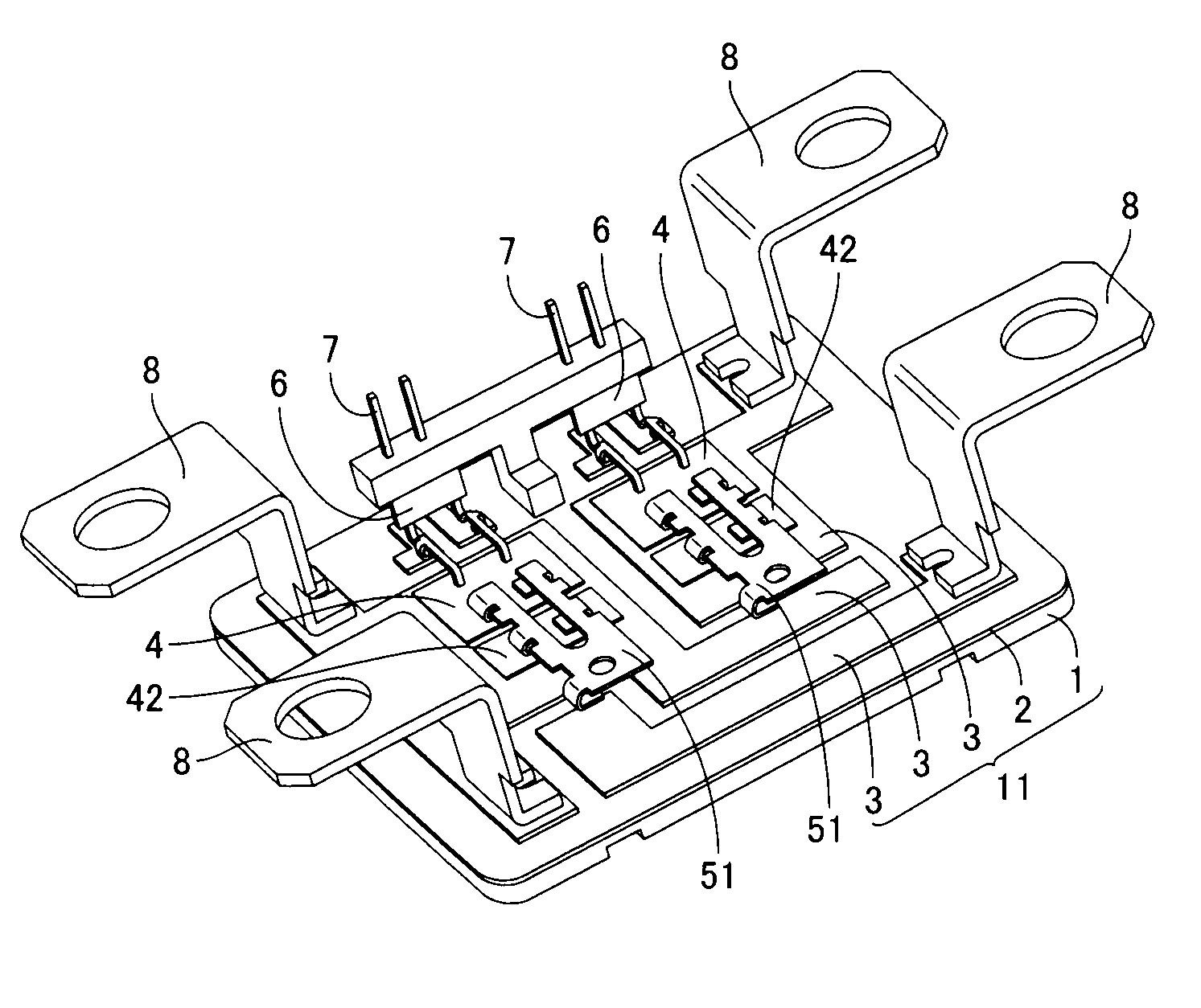
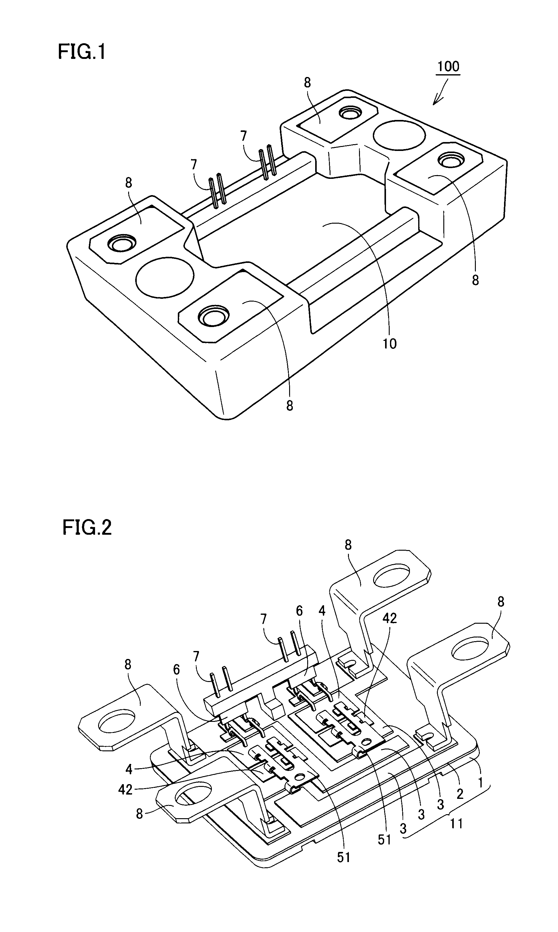
[0026]Referring to FIGS. 1-4, a semiconductor device 100 of the present embodiment has a substrate 11, semiconductor elements 4 and 42, an electrode lead 51, a sealing resin portion 10, a signal lead 6, a signal terminal 7, and a main terminal 8.

[0027]Each of semiconductor elements 4 and 42 is electrically connected to a circuit pattern 3 by electrode lead 51 and signal lead 6. Furthermore, semiconductor device 100 is connected to the outside by signal terminal 7 and main terminal 8. Among electrical paths formed in such a manner, a path connecting main terminals 8 to each other via semiconductor elements 4 and 42 as well as electrode lead 51 serves as a path for a main current of semiconductor device 100.

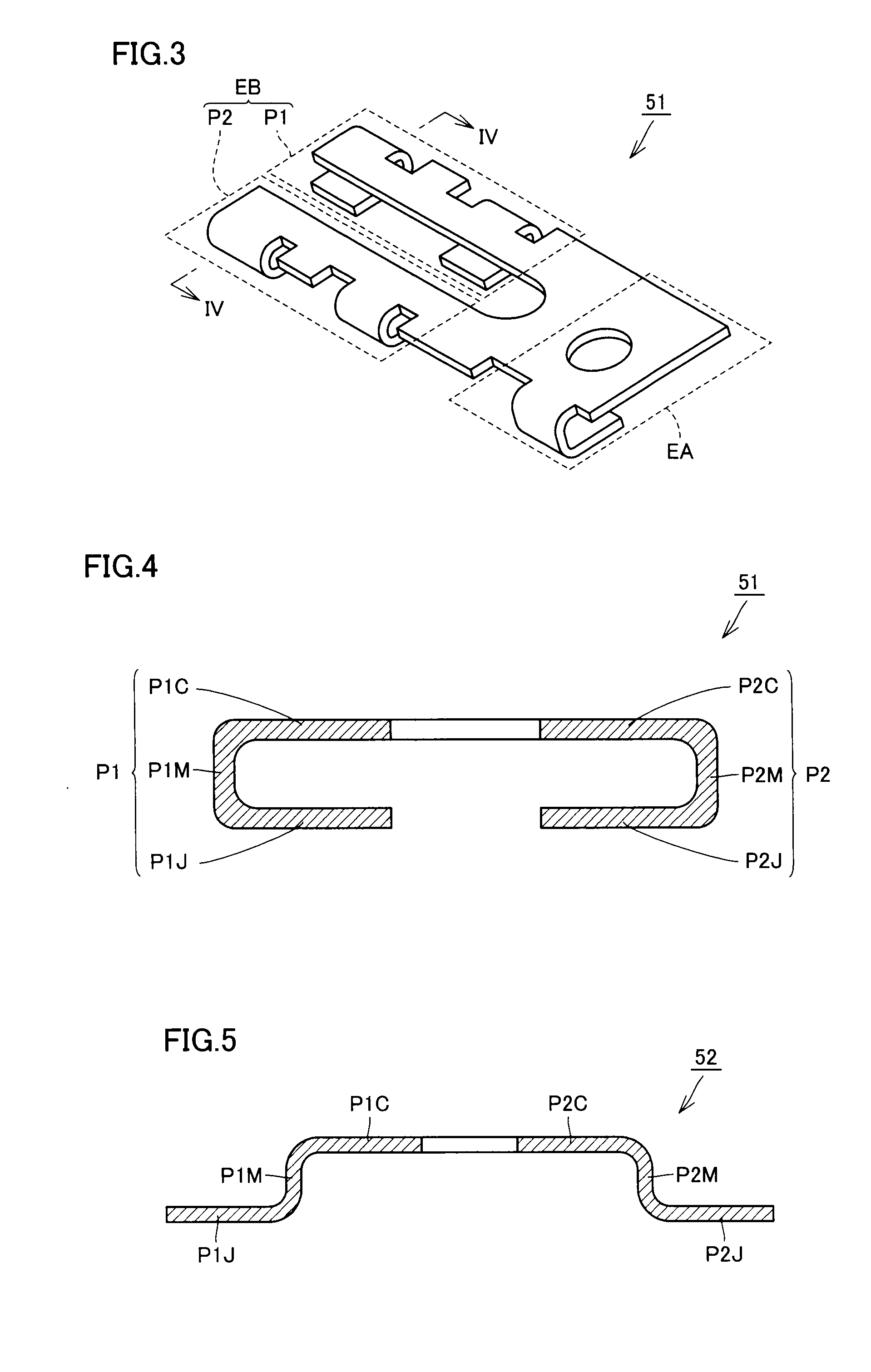
[0028]Substrate 11 has a base plate 1, an insulating layer 2 and circuit pattern 3. Insulating layer 2 is formed on a main surface of base plate 1. Circuit pattern 3 is formed on insulating layer 2. As a result, substrate 11 has a main surface (a surface shown in FIG. 2) on which c...

Login to view more

PUM

No PUM Login to view more

Abstract

A semiconductor device has a substrate, a semiconductor element, an electrode lead, and a sealing resin portion. The substrate has a main surface on which a circuit pattern is formed. The semiconductor element has first and second surfaces, and is arranged on the substrate such that the first surface faces the main surface. The electrode lead has one end joined to the circuit pattern and the other end joined by soldering to the second surface. The other end has a plurality of portions divided from each other. The sealing resin portion seals the semiconductor element and the electrode lead. Thus, there can be provided a semiconductor device that has relieved thermal stress at a joining portion of the electrode lead, and therefore is less subject to fatigue failure.

Description

BACKGROUND OF THE INVENTION[0001]1. Field of the Invention[0002]The present invention relates to a semiconductor device, and in particular, to a semiconductor device having a sealing resin portion that seals a semiconductor element.[0003]2. Description of the Background Art[0004]Semiconductor devices include a power semiconductor device having a mold resin (sealing resin portion) as disclosed in Japanese Patent Laying-Open No. 2003-264265, for example. According to this publication, the power semiconductor device has a semiconductor element, a metal block, a lead frame, and a casing. The semiconductor element has a surface and a back surface. The metal block is fixed to the back surface of the semiconductor element. The lead frame is fixed by soldering to the surface of the semiconductor element. The semiconductor element, the metal block and the lead frame are integrally-molded by the mold resin of the casing.[0005]The foregoing publication describes that, according to a configurat...

Claims

Login to view more

Application Information

Patent Timeline
no application Login to view more
IPC IPC(8): H01L23/495
CPCH01L23/3107H01L23/3735H01L2924/00014H01L2924/01068H01L2924/01033H01L23/49524H01L23/49531H01L23/49811H01L24/36H01L24/40H01L24/45H01L25/072H01L2224/45124H01L2924/01013H01L2924/01014H01L2924/01029H01L2924/0106H01L2924/01074H01L2924/01082H01L2924/19043H01L2924/01005H01L2924/01006H01L2924/01019H01L2224/48H01L2924/351H01L2924/181H01L2224/40225H01L2224/37011H01L2224/84801H01L24/37H01L24/84H01L2924/00H01L2224/37099H01L2224/73221
Inventor YOSHIDA, HIROSHIOTA, TATSUOTANIGUCHI, NOBUTAKESUDO, SHINGO
Owner MITSUBISHI ELECTRIC CORP
Who we serve
  • R&D Engineer
  • R&D Manager
  • IP Professional
Why Eureka
  • Industry Leading Data Capabilities
  • Powerful AI technology
  • Patent DNA Extraction
Social media
Try Eureka
PatSnap group products